Accelerating the green energy transition
Photovoltaic or solar cells are semiconductor devices that convert sunlight into electricity. Today crystalline silicon and thin-film silicon solar cells are leaders on the commercial systems market for terrestrial applications. The article describes the basics of traditional technology, developed in Ukraine in 2001-2005 and implemented into production.
Photovoltaic cells or solar cells — these are semiconductor products that convert sunlight into electricity. There are different technologies of solar cells, the design of which is distinguished as the physical principles of conversion of solar radiation into electric current and less important details. Most effective in terms of energy, devices for converting solar energy into electricity are semiconductor photovoltaic cells (solar cells), as it is a direct, one-step transfer of energy. Today the market of commercial PV systems for terrestrial applications are most noticeable crystalline silicon (about 80-85% of the world market) and thin-film solar cells (about 10% of the market). Next we’ll talk about the production of crystalline silicon solar cells, which are a key component of solar panels.
Solid-state solar cells
Solar cells are one of the most affordable and durable, what is more energy-balanced, alternative energy sources. The implementation of solar cells is usually based on solid-state technologies and is generally well-worked. For the first time, the photovoltaic effect was obtained in 1941, and the first solar cell was created in 1954 on the basis of a diffusion silicon p-n transition. Subsequently, solar cells were developed and created on the basis of other semiconductors using different designs.
While choosing the source material for solid-state solar cell, at first it is necessary to take into account the width of the bandgap of the semiconductor, which determines the maximum specific power of the photoconverter. At present, the following semiconductors are the most suitable for the manufacture of solid state electrodes: silicon (Si), cadmium telluride (CdTe), gallium arsenide (GaAs) and indium phosphide (InP).
Today’s solar cells can be classified on the basis of the quantity for their manufacture of materials, which are divided into crystalline and thin film, polycrystalline or amorphous.
Solid-state crystalline materials primarily include monocrystalline and multicrystalline silicon, grown by the method of pulling through filer profiles of silicon, dendritic silicon tapes, gallium arsenide. Thin film materials include semiconductors grown on electrically active or passive substrates, namely amorphous silicon, cadmium telluride, copper dyselenoids and indium.
Solid-state silicon solar cell became the most widespread, as the spectral characteristics of silicon absorption are well consistent with the spectral characteristics of solar radiation. With the help of silicon, it is possible to convert into electricity about 91% of the energy of the incident light flux, that is, part of the solar spectrum with a wavelength of 1.1 microns and shorter.
Solar cells based on crystalline silicon have a fairly high cost, primarily associated with the expensive operation of cutting silicon ingots into plates. Silicon solar cell has a theoretical marginal efficiency of about 30% under standard conditions (1 kW / m2 illumination, + 25 ° C, air mass AM1,5).
Amorphous silicon acts as a cheaper alternative to crystalline silicon. Optical absorption of amorphous silicon is 20 times higher than crystalline. Therefore, for a significant absorption of visible light an a-Si: H films thickness of 0.5 … 1.0 microns is enough instead of expensive silicon 240 micron substrates. In addition, for the production of amorphous silicon in the form of thin films of a large area, it is not necessary to perform a cutting operation, which is required for a sollar cell based on monocrystalline silicon. All these things reduce the cost of silicon by 20 times. The maximum efficiency of the solar cell based on a-Si: H is slightly lower than the efficiency of the crystalline silicon sollar cell and in theory can reach 16%.
Quite promising material, which attracted the attention of a large number of researchers, is gallium arsenide, with which it was immediately possible to obtain a fairly high efficiency. Despite some disadvantages (fragility, high density), gallium arsenide has undoubted advantages over silicon. Given the large Eg width, its ability to convert a long-wave radiation is limited (it absorbs radiation with a wavelength less than 0.9 microns), but it also leads to significantly lower values of reverse currents (10-9 … 10-10 A / cm2 versus 10- 6 … 10-7 A / cm2 in silicon FEP), and also makes it possible to obtain large values Uxx = 0.7 … 0.8 in a rather high efficiency. In addition, solar cells from there are characterized by a slower drop in efficiency with increasing temperature and increased absorption capacity of solar radiation.
Silicon solar cells
Solar cells are semiconductor products that convert solar radiation into electrical current. There are various technologies for the production of solar cells, the construction of which differs due to physical principles of transformation of solar radiation into electric current, and less essential details. The most effective, from an energy point of view, devices for converting solar energy into electric one are semiconductor photovoltaic converters, since this is a direct, one-step energy transition. Today in the market of commercial systems of ground application, the most notable are crystalline silicon (about 80-85% of the world market) and thin-film solar cells (about 10% of the market). Next we will talk about the production of crystalline silicon photoconductors, which are a key component of solar modules.
Chemical processing
The most important and most expensive part of any solar cell is a silicon plate. It can be both monocrystalline and multicrystalline. From the name it is clear that monocrystalline plate is a single crystal, from which, for example, by wire cutting one receives silicon plates of required thickness and size. Usually monocrystalline is grown in the form of round ingots, from which then cut the so-called pseudo-quadratic plates. This form provides maximum use of silicon from a round ingot and, at the same time, the densest filling of the surface of the future solar module (solar cell). Multi-silicon plates are the right squares of a given size and thickness.
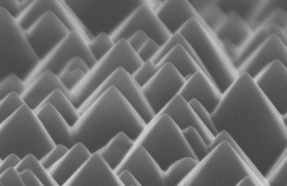
Since each plate has a surface damaged while cutting bars at the nano level, this damaged layer must be removed. If just a few microns remove by chemical etching, the surface of the plate will be smooth and reflect a substantial portion of the incident radiation. In order to obtain more efficient solar cells it is important to convert as much sunshine as possible into the current, the surface is tried to make it unequal at the micro level. Monocrystalline plates for such process operation are called texturing.
The textured surface is seemingly a set of randomly distributed micro pyramids. The light on the surface of the pyramid, is reflected at the same angle and in most cases falls on the brink of a neighboring pyramid. Thus, only by creating a textured surface one can reduce the reflectance of silicon from 35% to 11%.
To solve both mentioned problems (removal of the damaged layer and the formation of the texture on the surface of the plates) used wet chemical processing plates. The complexity of solutions, temperature and duration of treatment depend on the type of processed plates, the surface condition before the treatment, further processing operations and many other factors. Typically, plates are used for monocrystalline etching in alkaline solutions and one or more acid treatments. At the same time it is important not to overdo, as in pursuit of uniform surface texture it can significantly reduce the thickness of the plates. This will lead eventually to increased battle on subsequent operations and, as a consequence, to decreasing of product yield percentage .
At the end, after all the necessary operations, the plates are rinsed in water and dried. These are also very important operations. For example, the quality is depended very much on the drying characteristics of the diffusion layer produced by the following operation.
The heart of the solar cell
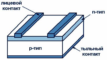
A key element of the design of crystalline silicon solar cells is a p-n junction. What is it? It is the fact that a semiconductor depending on their conductivity type may be either n-type (electron conduction), and p-type (hole conduction). At the same time, if to create a layer of another type of plate , the point of contact of these areas will be a p-n junction. Generally p-n junction is one of the key concepts of solid-state microelectronics. With the use of physical effects, occurring in or around it, such all known products as diodes, transistors and many other more complex chips work.
One of the main characteristics of the p-n junction is its ability to be an energy barrier for the charge carriers, i. e. they pass only in one direction. Exactly with the help of this effect the generation of electric current in solar cells is based. Radiation falling on the surface of the element, in the semiconductor generates charge carriers with different signs — electrons (n) and holes (p). Due to its properties the p-n junction «shares», skipping each type only on its “own” half, and chaotically moving in the volume of the element charge carrier are detected on different sides of the barrier, after which it can be transmitted to the external circuit to generate the voltage on the load connected to the solar cell.
Of course, this description is a bit simplified, but even it shows that without the p-n junction it is virtually impossible to convert solar radiation into electric current (remember that we are talking about the classic terrestrial solar cells, and in fact there are more exotic photovoltaics, design does not imply the existence of p-n transition). So how it is possible to form a p-n junction?
As we already know, original plate undergo several stages of chemical processing at the very beginning, thanks to which fact their surface acquire necessary for us structure and purity. Typically in the manufacture of solar cells p-type conductive plates are used. For this step a further silicon ingot doped with appropriate cultivation impurities, e. g., boron. Therefore, to create a n-layer it is necessary to introduce another impurity element in one of the surfaces which compensates the effects of boron and saturate a semiconductor by n-type charge carriers. It can be done by introducing phosphorus in silicon or other suitable admixture of the relevant part of the periodic table.
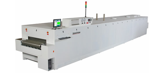
One of the most traditional and economically reasonable ways to fill silicon is phosphorus diffusion, i. e. a process in which phosphorus at high temperatures penetrates into the semiconductor. Traditionally, diffusion of phosphorus is carried out in tubular furnaces or conveyor at temperatures around 800 oC. In the first case, the quartz plate is placed in the cassette, and the tube furnace is filled pairs substance containing phosphorous. Handling the time spent of plates in the reactor, its temperature and gas flows within it, technologists receive a p-n junction with the necessary properties to them. In other case, the phosphorous material is sprayed onto the surface of the plate lying on a conveyor belt furnace. Thereafter the plates are moved using the conveyor to the next zone, which is also subjected to high temperature treatment.
As a result of the diffusion of phosphorus on the surface of the silicon plate and the ends of a thickness of about 200 microns, a layer of n-type is formed, penetrating to a depth of only about 0.5 microns. That is a p-n junction occurs at the surface of the solar cell. It is done to ensure that the charge carriers of different signs generated by the radiation were in the area of influence of the p-n junction as quick as possible, otherwise they will meet again each other and thus balanced by, and to prevent any contribution to the generation of electric current.
Plasma etching
The construction of a solar cell requires a p-n junction near to one of its surfaces, which is called the front or working side. The other surface is called back. Typically located on the front surface is a current collecting grate, and rear-solid contact. Since the n-layer is formed by diffusion, heavily saturated with impurities, it is a good conductor of electric current. During this diffusion layer it is formed not only on the front side of the plate, but at its end and even on the rear surface of the perimeter. Here we have the electrical circuit between the front and back current collecting contacts.
Typically, this problem is solved by physically removing it from the ends of the plates. It can be done mechanically, laser, chemical or by plasma etching. Without going so far in the analysis of the advantages and disadvantages of each of these methods, it can be said that one of the most rational of them is still the plasma etching. Operation is a plasma processing stack tightly pressed against each other silicon plates. The process of removing the silicon depends on many characteristics, among them — the duration of treatment, the plasma composition, the direction of flow of ions in the reactor location and tightness of the plates, the size of the stack, and others.
If you deviate from the optimal regimes there may be two opposite results:
- n – the layer at the ends of the plates is not removed, which leads to the closure of the solar cell on the ends after the formation of the contacts;
- n – the layer is removed not only at the ends of the plate, but also along the perimeter of the front and back surfaces, that is, the closure occurs in the place of contact of regions with different types of conductivity on its front side.
Monocrystalline plate baited on the face after plasma etching as follows:
In the first case, the problem can be solved by controlling the conductivity type at the ends of processed plates. The second case is more complicated — spoiled electric characteristics and the appearance of the front surface require full bleed n- layer, and only thereafter can be sent again to the initial processing steps. At the same time, repeated texture leads to a decrease in its thickness, that is, the growing battle of plates in subsequent operations. Additional processing and reduced output of suitable products lead to increased costs and substantially impair the economy.
Antireflection coating
Thanks to the surface texture the reflection of the plate is reduced from an average of 35% to 11%. It means that one tenth of the radiation incident on the surface of the solar cell, will still be reflected back and will not participate in the generation of electric current. In order to reduce these losses further, that are classified as optical, for the next machining operation on the working surface of the solar cell a so-called antireflection coating (ARC) is applied. Based on the laws of optics, engineers select thickness and refractive index of the coating, so that we can reduce the reflection up to 1-2%. And this is a very good indicator.
Today there are so many different types of anti-reflection coatings, which are applied by several different methods (APCVD, LPCVD, PECVD, etc.). In practice, as ARC for silicon solar cells are most commonly used titanium oxide film or silicon nitride, the last one being is increasingly preferred. Silicon nitride is usually applied by PECVD, i. e. by accelerated plasma chemical deposition from a gaseous phase, in special tube furnaces.
PECVD process supposes that the chemical reagent zone entering the reactor decomposes under the influence of plasma and temperature on the individual elements which are then deposited on the plate surface and react chemically. As a result, on the front surface of the plate it is « grown» thin film of silicon nitride which has the desired properties. Its thickness is about 70 nm, which is much smaller than the micropyramid texture and it allows to achieve antireflection effect regardless of the surface relief structure.
This method provides a very good uniformity of the coating. To estimate the thickness of ARC is quite easy. Optics is such that the more thickness is uneven, the greater the coloring surface of the plate is changed. The same effect can be seen looking at a puddle of spilled gasoline — film shimmers with all colors of the rainbow, making it clear how changing its thickness. Other known methods of applying ARC often require a preliminary application of the solution on the plate surface, which cannot be done uniformly (substance will accumulate in «leaves» between micropyramids and will not dwell on their tops). It also finally affects the appearance of the solar cell deteriorates and its parameters.
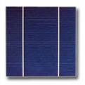
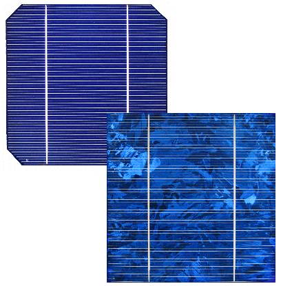
After applying ARC a silicon plate absorbs a large part of the solar radiation incident upon the surface. Moreover, coating thickness is optimized such that run most efficiently in the most efficient range of the spectrum. We are going to devote a separate publication of this issue a bit later, and now I can only say that it is the blue part of the spectrum. It is because of the fact that all solar cells have beautiful and deep navy blue color.
After applying ARC a solar cell is almost ready. Under the influence of radiation inside the device it is already happening the generation of charge carriers, which are then separated p-n junction and almost ready for use. But they need to pass into the load circuit, and for this passing it is necessary to form a contact surface of the solar cell.
The front contact metallization
The front surface serves at first for maximum absorption of the radiation on it, and it defines the technical requirements for the contact metallization. It is for this reason the contact located on the working side of the solar cell is performed in a grid, usually consisting of 2-3 wide pads and several dozen thin current collector lines perpendicular to the broad.
When choosing the design, engineers have personal contact to solve two conflicting aims. Firsty, to reduce the optical losses due to shading metal work surface, they try to perform the grid lines as thin as possible and place them as far as possible from each other. Secondly, since the surface of the element has a specific electrical resistance (defined modes of formation of the p-n junction by diffusion), at a very great distance between the contact elements of the lattice part carriers simply do not have time to reach the contact and recombine inside the semiconductor material. Therefore, in order to reduce electrical losses with a given surface resistance plate the space between the lines of the contact grid can not exceed a certain value. The same goes for the width of the lines — the thinner the line, the better optics is, but the less current will be able to hold such a contact. Plus the very method of forming metallization has its limitations on the minimum line width. For example, the contact width of 125 microns is quite simple and inexpensive to do, and the contact width of 80 microns — it is the fate of laboratories and enthusiasts.
Usually, in order to reduce the cost of solar cells, contact metallization is applied by screen printing or as it is called — silkscreen. The essence of this method is that by using the so-called squeegee (if very simple, the rubber bar) through a fine mesh stencil pressed paste, composed of metal balls, flux, and various binding agents. On the preformed grid pattern defining places where the paste is to be applied to the plate, and in which — no. After this paste is dried, the plate enters the furnace of brazing, where at temperatures above 800 degrees baked into the metal surface in a solar cell.
Since the paste contains enough solid components, to increase the stability in the manufacture of solar cells stencils formed by metal meshes are used. The width of the thin lines of contact metallization puts demand on the screen characteristics, which typically can be from 165 to 325 openings per inch. It allows you to get in the end contact width 125 mm, located at the desired location with a positioning accuracy better than 10 microns. More detailed method of screen printing stencils and stencils themselves, we are going to look through later.
For the formation of the front metallization of solar cells, today complex composition containing silver paste is used. Type of paste and its properties are very important to obtain good parameters of the finished product. According to our evaluation, for only a few years due to technological improvements pastes, the producers managed to raise the efficiency of solar cells by 1-1.5%. And taking into account the efficiency of conventional silicon terrestrial element now lies in the range 15-17%, such an additive is more than essential.
Besides the above-mentioned problems in the formation of the front contact metallization, I cannot but mention another important point. As it was said above, p-n junction lies at a depth of about 0.5 microns. While brazing with silver paste, the metal must enter as much as possible in the n-silicon layer, but it does not reach the p-layer. Otherwise there will be a electrical contact between two types of semiconductor and solar cell would be short-circuited. This requirement complicates the task of brazing paste, which must penetrate into the plate with a truly exquisite accuracy. For this case the thermal treatment is carried out in special high furnaces, providing the peak effect on the plate for a time of about 10-15 seconds.
Of course, many manufacturers use the old-fashioned slow conveyor ovens, in which the plates are in the area burning in about 3 minutes and also get acceptable characteristics of products. But the transition to the use of high-speed furnaces can increase the efficiency of the solar cell at least 0.5%. And this is a significant advantage in the total capacity of products produced per year.
Backside metallization
Unlike the front metallization that serves only contact metallization, the back one solves another problem. Usually on the back surface of the solar cell is put not one, but two types of metal. One of them is a continuous aluminum layer covering substantially the entire area except for a few holes. And in these holes the silver plating has already formed , performing the function of the contact.
Why do I need an aluminum layer? The fact that it serves as a mirror for the charge carriers. But not the optical mirror and energy. As it is well known, electrons and holes in semiconductors tend to recombine, i. e. move from free to bound. Recombination occurs, for example, if at one point there are two different charge signs. One of the extreme cases is the so-called surface recombination because any surface is a set of dangling bonds of the crystal lattice — «traps» for the free charge carriers. It is in order to reduce the impact of this type of recombination in solar cells with aluminum metallization formed the so-called BSF (back side field) — «reflect» carriers, which have not yet give a contribution to the current generation.
The aluminum layer on the back side provides a solar cell of a few tens of mV higher voltage than it would have been without it. I. e. 24 in case of solar cell, this additive is at least 0.5, which corresponds to around 2% increase in capacity. That is how engineers little by little increase the efficiency of solar panels, making it more efficient.
As the silver-containing contact and a continuous aluminum layer on the back side of the solar cell are formed in the same screen printing method. Drawing stencil and some characteristics utilized in the grid only change. For example, due to the size of aluminum particles in the ink have to be used with larger mesh cells in comparison with grids for applying silver pastes. Also the taut wire differs and some other process characteristics. After application of each layer of the paste it is dried in ovens, and only after the application of the three layers (one on the front and 2 on the back side) is transmitted to the sheet by heating.
In general, the process of screen printing is very complicated and requires experience of all participants — engineers, servicemen and operators. For example, viscosity and other properties of the pastes extremely depend on the temperature and humidity in the shop, draft, etc. Changes in the indoor temperature even at 2-4 degrees requires cumbersome reconfiguration process. Also affect the outcome terms and conditions of storage of pastes, state squeegee, printer settings, and even the characteristics of the air supplied to the furnace brazing. Particularly it is difficult to reconcile all of these options because the formation of metallization — this is the last operation and the plates had gathered all the deviations from previous operations. That is why all dimensions and other plates characteristics differ in the party much more than in the first step, and tunes in to the optimum so much harder. But all the effort worth it, since the output we get finished solar cell, which remains the only measure in the future, sort and pack the characteristics.
Testing
Obviously, any article of manufacture prior to delivery must be carefully checked and measure its parameters. Do not avoid this procedure, and in the manufacture of solar cells.
The first solar radiation characterized parameters such as the intensity, i. e. power incident on the surface of a certain area. This parameter vary in different regions of the Earth; the maximum intensity of solar radiation on the planet exceeds 1300 W per square meter, but for convenience in measurement, a standard value at a level of 1 kW / m. m
Another important parameter is the distribution of solar radiation by wavelength, i. e. spectral composition of light. To characterize it, the concept of «air mass» is introduced (AM — Air Mass): so the spectral composition of the radiation from the air mass corresponds AM spectrum of sunlight outside the earth’s atmosphere; AM1 corresponds to radiation at the Earth’s surface, in case that the sun is directly above the point of observation, ie rays of light passed through the 1 atmosphere; corresponding to solar radiation, which took 1.5 atm.
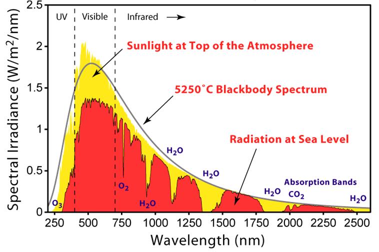
The final condition of the standard measurements of solar cells is the temperature. The fact that the characteristics of this product somehow reduced when the temperature rises, so it is very important that it has not changed during the measurements. Standard assumed that testing is performed at 25 degrees Celsius.
During testing of the solar cell measure the set of parameters, including short-circuit current, open circuit voltage, maximum power and the efficiency. Setting the maximum power of the solar cell efficiency provides an answer on the question raised at the beginning of this article and shows what part of the incident power will lead to the emergence of electric power to the load.
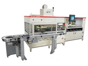
For precision measurements of solar cells testers or testers / sorters are used. They can be both pulsed or continuous irradiation. Pulse testers interesting because during almost instantaneous the measurement element could not heat up and the error below. Testers also differ in the type of lamps, which affects the spectral composition of the radiation.
Usually the tester contains a reference solar cell and built-in computer, which converts the measured characteristics and brings them to the standard conditions of measurement. At first glance it seems that the measurement is a fairly simple task — you just need to change the voltage and measure the corresponding currents. However, in reality it is necessary to consider a number of additional factors, among which the most important are the following:
- Since the generated current is directly proportional to the element of light, it must be accurately known and constant.
- It is necessary to achieve high uniformity of light on the surface of the test element.
- The spectral distribution of light should be as close as possible to the spectral distribution of natural light.
- You must know the temperature being measured.
- It is necessary to eliminate any voltage drop at the contacts and in the chain, which introduces additional errors in the measurements.
To ensure uniformity of radiation, there are two most common ways: use special optics with reflecting and diffusing elements or use a point source of radiation. In the first embodiment, it is often necessary to control and configure the hardware, and to compensate the influence of the reflector and other optical elements on the spectral distribution using an additional filter, which leads to great difficulties in use. In the second embodiment, the desired uniformity is achieved by diversity of the source and the test image to a considerable distance. Most common in the industry are pulsed xenon lamp testers.
So, there were the fundamentals of traditional technology developed in Ukraine and introduced into production mentioned above. It was probably the most common technology for creating silicon solar cells with contacts deposited by screen printing. As it may seem, the production process of photovoltaic cells is quite simple compared to traditional microelectronics products. But it is only at first glance. In fact, in the technology of solar cells there are so many difficulties and pitfalls.
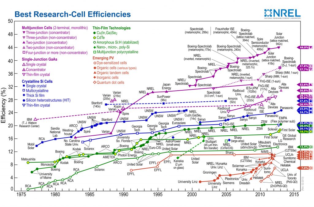
Below you can find a visual illustrating of the latest achievements in the efficiency of photoelectric solar cells manufactured using various technologies.
Solar panels for space and ground applications
The problem of the development of solar energy is currently attracting the attention of specialists of various scientific disciplines. Particularly great successes have been achieved in creating semiconductor solar cells and batteries of various designs. Increasingly, lighter and more powerful solar panels of spacecraft and stations are becoming increasingly widely used on the ground, all above efficiency and more diverse their properties.
The development of the theory and experience of past years allowed to describe the physical mechanisms of the photoelectric effect, to determine the sources of power losses in the solar cells, to explain the gained actual efficiency and to indicate the ways of their increase. The zone theory of solids in conjunction with the thermodynamics of the semiconductor-radiation system made it possible to make an optimal choice of the semiconductor output, introducing the concept and determining the value of the boundary theoretical efficiency. And although it has not always been possible to bring the level of knowledge to understanding all the complex electronic processes occurring in the volume of the semiconductor or on its surface – contacts with air, metals or other substances. However, it usually turns out how it is possible to avoid the effects of negative phenomena, to strengthen the role of positive and to develop models of improvement.
Unusual operating conditions (weightlessness, deep vacuum, contrast temperature changes) do not allow us to use widely space-known traditional methods of obtaining electricity on Earth. Therefore, the main source of electric power for spacecraft is solar panels. And the development of space technology requires further improvement and increase of technical and economic indicators of the latter. Work in space presents SE with very rigid and sometimes contradictory requirements. Indeed, absorbing at most light energy, they should not overheat. While diodes and transistors are placed in hermetically sealed, sometimes heat-insulated device compartments, the panels of solar cells are heated to +80 ° C when they are illuminated by the Sun, and cooled to -150 ° C during the onset of space vehicles in the shadow of the Earth. In addition, solar panels should have the ability to resist the fluxes of corpuscular radiation, the effects of high-energy particles and meteorite streams for a long time.
But no less tough requirements are imposed on photovoltaic converters exploited in ground conditions. This is due to the growing spectrum of the use of solar batteries in Ukraine. Initially, solar panels were used only in portable appliances, with a low lifetime and low power consumption. Currently solar cells are used as stand-alone power supplies for navigation and communication systems, telecommunication and additional power sources that operate at peak load times in the grid. These energy sources should have high power, long service life and weather resistance. The same solar cells should be inexpensive and have the ability to connect to large batteries.
The most widely used become the silicon solar cells, due to well-developed technology, relative cheapness of raw materials and good characteristics of silicon in terms of direct conversion of solar energy into electricity. The main directions of characteristics improvement of solar cells are: optimization of parameters of existing converters, improvement of technology of manufacturing of solar cell in order to reduce the material and energy costs for their manufacture, the use of new materials in the technology of solar cell. We will write about this and not only many times later.
Impact of defects on the quality of solar cells
In the semiconductor materials which are used in the production of photovoltaic converters, defects of different types occur first, depending primarily on the method and conditions for obtaining the semiconductor. The activity of defects is determined by their type, the size in the field of deformation, the interaction of defects with each other and with impurities, the location of defects in relation to the active regions of the solar cells, the type and characteristics of the production of solar cells.
Different thermal and mechanical processes that take place at all stages of the manufacture of solid-state solar cells, can lead to the appearance of new structural defects, as well as additional impurities in the treated material. In addition, in course of technological operations it is possible to change the nature of existing defects and the development of new defects. Defect formation at each stage of the technological process also strongly depends on the previous operations and modes of further operations.
Structural defects significantly affect the lifespan of the charge carriers and the resistivity of the material, which lead in the result to changes in the voltamper characteristics of the solar cell. Defects cause an increase in leakage currents, lead to a local breakdown of the p-n transition, the heterogeneity of the diffusion front of impurities, the breakdown of metallization, punctures of oxide, which in turn leads to degradation of solar cell, as well as a decrease in the percentage yield of suitable products and their reliability.
Defects in the installation of silicon solar cell
The source defects of the structure of the solar cells include agglomerations of point defects, dislocations and their accumulation, planar defects of the type of double, defects of packaging, grain boundaries, as well as precipitates and microdefects, which are located inside the grains, macrodefects of the material, etc. Deviations, in course of technological operations, surface contamination and volume of semiconductor material, liquid and gaseous process environments, thermal and mechanical processes also lead to the emergence and development of defects associated with imperfection of the design of solar cell.
The following types of structural defects of silicon solar cell were found in the research samples: structural defects and surface contamination of silicon plates, defects in the anti-reflective coating (ARC) structure, uneven depth of occurrence of the back isotypic transition, mechanical bits on the perimeter of the plates, defects in contact metallization.
The remnants of the broken silicon layer lead to an increase in the speed of surface recombination and a decrease in the spectral response of the solar cell. The uneven height of a pyramid of a texture may cause unevenness of the thickness of the ARC and, accordingly, increase the integral coefficient of optical reflection from the surface of the solar cell. The presence of metal particles and other contaminants on the surface of the plates leads to the ejection transition.
Cracks and pores in ARC arise during high-temperature plate adjustments due to the difference in coefficients of thermal expansion of the coating material and silicon. These defects lead to a decrease in the optical transmittance of the ARC and an increase in optical losses.
The unevenness of the depth of the back isotypic transition occurs when the suboptimal or unstable modes of application and incineration of aluminum on the back surface of the solar cell. Reducing the depth of the back isotypic transition leads to an increase in the rate of recombination at the back of the plate and to reduce the idle speed of the device.
Mechanical bits appear when the plates are contacted with technological equipment, tweezers, etc., as well as due to inappropriate manipulations with plates. Mechanical bursts cause the formation of microcracks in plates, which lead to a significant degradation of the electrical parameters of the solar cell.
The defects of contact metallization include:
- discontinuities and unevenness of the width of the silver contact tire, unpublished areas and the deviation of the pattern of metallization due to defects of the stencil when the contacts are applied by the screen printing method;
- uneven thickness of metallization;
- absence of adhesion of the face or back contact metallization as a result of deviation from the optimal modes of ignition and contamination on the surface of the plates;
- datachment and disruption of aluminum metallization due to the difference in coefficients of thermal expansion of silicon and aluminum.
Defects in contact metallization lead to the mechanical pressure on plates, a decrease in the short-circuit current density and the impossibility of connecting the solar cell in the module to obtain the specified values of current and voltage at the operating point.
Energy loss reduction in the ground-based solar cell
To reduce the optical losses dealing with the use of photovoltaic radiation converter reflected , the most widely used methods now are:
- surface structuring, which leads to a decrease in the integral coefficient of the solar cell display;
- application to the surface of the solar cell single- or double-layer anti-reflective coating;
- reducing the area of contacts on the front surface to reduce shading losses;
- application of a metallic layer to the back of the solar cell, which increases the efficiency of the absorption of long-wave radiation due to its multiple passage through the volume of the semiconductor;
- reducing the depth of the emitter transition and reducing the concentration of the doping admixture near the front surface to increase the sensitivity of the solar cell in the short-wave part of the spectrum.
Electric energy losses are usually reduced by the following methods:
- the choice of the optimal step and the thickness of the contact tire on the front surface to reduce the successive resistance of the solar cell;
- the use of gettering treatments that increase the lifetime of non-main charge carriers;
- passivation of the facial surface to reduce the rate of surface recombination;
- passivation of the back surface and creation of isotypic transition;
- minimization of the contact area and additional doping of the contact areas to reduce the recombination losses at the boundary of the metal-semiconductor section.
Below you can see a graphic diagram illustrating the latest advances in the efficiency of solar cells manufactured using different technologies.
Read more:
Some features of designing BIPV-systems
In this article we will talk about the features of designing BIPV-systems - both from an architectural point of view, and from the position of calculating an integrated solar power station, as well as the multifunctionality of BIPV-elements.
Changes in world energy are inevitable
Data on the development of world energy, including renewable energy sources (RES), obtained in mid-2018, show that an important milestone has been reached - the generating power of energy from the sun and wind exceeds one terawatt
Generation forecasting from variable RES
Forecasting becomes a decision instrument for cost-justifiable integration of resources of variable renewable energy (VRE), such as wind and solar energy, into local, regional and national grids.
What area is required to build a solar PV power plant?
One of the issues that may arise when planning a future solar power plant is the required area for the mounting of solar panels.